COM Team – Projects
I. Doping of semiconductors
I.1. Localized doping
Doping of semiconductor materials is a key step in the fabrication of electronic components. Since component architectures are very complex, it is often necessary to dope the semiconductor locally (and not uniformly). The electronics industry mainly uses 3 techniques for localized doping: diffusion, ion implantation and in situ doping during epitaxial growth (with mask). In the case of wide bandgap semiconductors (SiC, GaN), the diffusion coefficients are too small, which excludes diffusion doping. Ion implantation is thus widely used but this technique is intrinsically limited by the depth of effective doping as well as by the generation of many crystalline defects that are very difficult to eliminate. Localized doping during epitaxial growth is also difficult because masks do not resist conventional epitaxial conditions. We therefore propose to use an unconventional growth technique to overcome this difficulty: Vapor-liquid-solid transport (VLS).
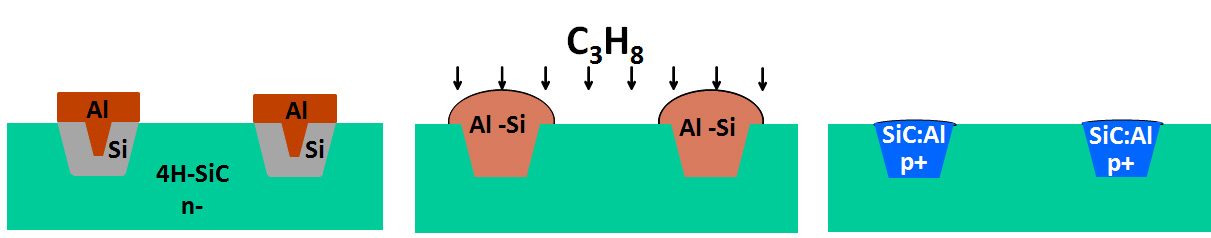
The aluminium serves both as a liquid phase for growth by VLS transport and as a p-type dopant for SiC. Thus, by optimizing the VLS growth conditions, we have demonstrated the achievement of localized crystalline deposits of 4H-SiC on areas of highly variable geometry. The deposited material is highly doped with aluminum ([Al] > 1020 at.cm-3). These layers are electrically tested to determine their potential to improve the performance of SiC-based electronic components.

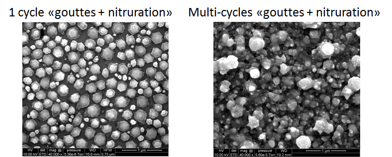
This approach of localized doping by VLS transport has been transposed to GaN, a material for which the doping problem is even more difficult. To do so, a network of Ga-Mg alloy droplets is first formed and then nitrided to obtain p doped GaN with magnesium.

I.2. New model for SiC doping
Electronic components (diodes, transistors) based on Silicon Carbide (SiC), allow a considerable reduction in energy losses during their operation, compared to silicon. SiC n type doping with nitrogen has long been controlled. However, despite the apparent maturity of this doping technology, the mechanism for incorporating N impurity into SiC during epitaxy is still far from being well described and understood. Starting from the numerous existing experimental results, we proposed (in collaboration with the LMGP Laboratory of Grenoble) a theoretical model of nitrogen incorporation into 4H-SiC during epitaxy.

This model is based on the dynamic exchanges existing between a solid material heated to high temperature and the gaseous atmosphere present during this heating. In the case of SiC heated under hydrogen at around 1500°C (usual doping conditions), the surface carbon atoms of SiC are etched by hydrogen, creating carbon vacancies at the surface. If a controlled amount of nitrogen is added to the gas phase, this element can then fill in the surface vacancies and thus be incorporated into the SiC crystal lattice. This dynamic surface exchange model could also potentially be applied to the determination of the incorporation mechanism of any impurity other than nitrogen into SiC. It could even be extended to the doping of other semiconductors. This work is published in the journal Scientific Reports and has been the subject of a communication on the CNRS website.
II. Atomic Layer Deposition
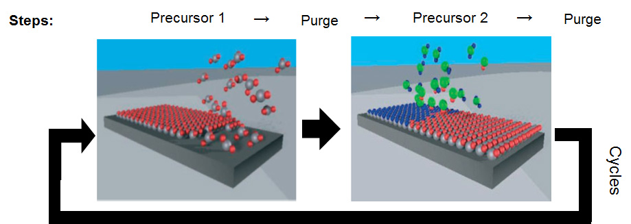
ALD (Atomic layer deposition) is the ideal technique for the deposition of conformal and homogeneous thin layers because of its simplicity and reproducibility. The principle of ALD is based on the reaction between different precursors introduced alternately and not simultaneously (unlike CVD). In this way each precursor reacts only with the growth surface which is ideally covered with a monolayer of the other precursor. The reaction process is therefore self-limited to surface reactions, which differentiates ALD from CVD.
II.1. Elaboration of an efficient BN textile for water treatment
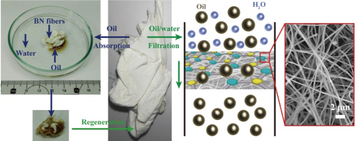
By adapting the “Polymer Derived Ceramics” route (low temperature deposition followed by heat treatment, developed by CIMP team) BN nanomaterials have been produced by ALD. The low deposition temperature thus attained has rendered possible the use of polymeric supports, which were not processable until now with “conventional” BN ALD (with ammonia and halide precursors). This process is therefore versatile and allows the manufacture of complex functional nano-heterostructures. Non-woven textiles, made of BN nanotubes with controllable internal diameter and wall thickness, were synthesized from electrospun PAN fibers (manufactured by the PSI team). These textiles show super-hydrophobicity and high stability against exposure to air and acid or basic environments. These textiles have proven to be excellent sponges and effective filters for organic compounds, property which can be used for water purification. In addition, they are easily regenerated by heat treatment under air and therefore reusable. Good repeatability of absorption and filtration experiments was observed. These new BN-based sponges are therefore very promising materials for water pollution control.
II.2. Heteroepitaxy of ZnO on GaN
ALD is intrinsically a “low temperature” technique, conditions for which epitaxy is difficult. For many applications, epitaxy of the layers deposited by ALD is not required. But in some cases, a highly oriented or even epitaxial layer is preferable, and the technique is then called ALE (Atomic Layer Epitaxy). We are studying in the COM team the epitaxy of ZnO on GaN by ALE to elaborate ZnO/GaN heterostructure that can be used for light emitting diodes or rectifiers. The precursors used are diethyl-zinc (DEZ) and water vapour (H2O). We periodically add trimethyl-aluminium pulses (TMA) for n-type doping of the ZnO layer.
